Introduction
Will of an Epoch
“Architecture is the will of an epoch translated into space.”
Ludwig Mies van der Rohe, the German-American pioneer of modern architecture, proved the above credo with glass-and-steel icons like the Seagram Building: stripped of ornament, built for an age that worshipped mass production. The will of Mies’s epoch — efficiency, mechanization, mass production — found its form in steel, glass, and concrete.
Mies wasn’t just addressing aesthetics, but diagnosing a deeper pattern: every generation translates its ambitions and aspirations into physical form. What gets built is never just a structure — it’s a mirror of the age’s intent.

So what is the will of our epoch? A hunger for intelligence. At scale. On demand. Everywhere.
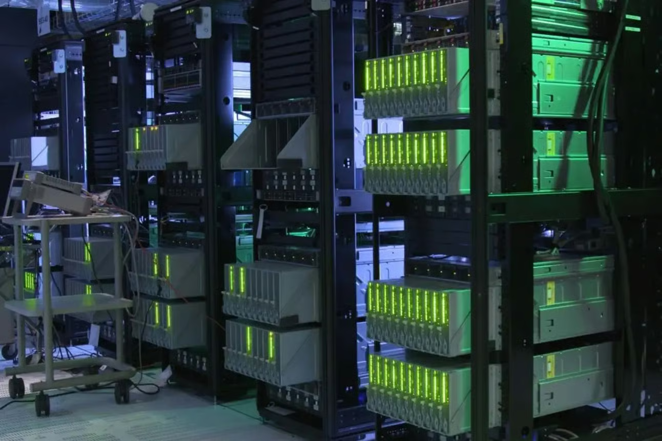
Today, we are building for artificial intelligence the way past civilizations built for industry, religions, and empire. We’re building cathedrals of compute, stacking racks upon racks of silicon, and carving new geographies of power corridors, fiber crossings, substation setbacks, and cooling plants.
And underpinning it all is a hidden architecture: the physical substrate on which intelligence runs.
That substrate is starting to change.
Electrons powered the last epoch. Photons may define the next.
We are living through an architectural movement. Or, at the very least, we really should be.
Section 001
The Electron Problem
“Every architectural revolution begins by admitting what no longer works.”
Our so-called cathedrals of compute — megawatt-scale AI clusters rising faster than suburbs in the Southwest, designed for model training runs that stretch across continents — aren’t metaphorical constructs. They are real, physical monuments to an age defined by the hunger for intelligence at planetary scale. But the substrate underneath — the humble electron — is straining under the weight.
Quick Reality Check: Other Escape Routes Exist
Photons aren’t the only way out of this cul-de-sac, and we’re not blind to the other exits. Before we sprint toward light, a nod to the two other escape hatches everyone keeps whispering about:
- Quantum computing
Uses superposition: each qubit can hold 0 and 1 simultaneously until measured, letting certain algorithms evaluate many possibilities in parallel. Great for factoring large numbers and simulating quantum chemistry. Today, though, qubits must sit at millikelvin temperatures and need heavy error-correction to tame noise. Hardware is domain-specific and power-hungry, so this is unlikely to be a practical engine for trillion-parameter LLMs this decade. - Neurotrophic hardware
Uses biomimetic design principles…the human brain is a hell of a piece of hardware! This field mimics neurons and synapses to promise brain-level parallelism on single-digit-watt budgets. Prototype chips exist, but large-scale fabs, mature tool-chains, and production ecosystems are still years away. Wide-scale deployment is highly unlikely over the next decade.
Both paths are important concepts, and will get deeper Per Aspera treatment later. Today, though, the focus is on photons.
AI’s insatiable appetite
GPT‑4, Gemini, and Claude aren’t just abstract codebases. These large language models map to cluster topologies, which map to physical interconnects, which map to how many electrons we can shove through copper before the system buckles.
A ChatGPT query uses ~10X more energy than a Google search. While trivial in cost per query…add scale into the mix, say 1B+ interactions daily, and AI already consumes ~3% of all U.S. electricity. This could triple within a decade. Across the U.S., datacenter-induced demand is already forcing hard choices: Northern Virginia, planet Earth’s densest server farm, will max out on power within two years. Meanwhile, in fast-growing markets like Phoenix and Dallas, operators are contending with significant challenges related to power availability and cooling — particularly in the Valley of the Sun, where water scarcity and extreme heat are forcing changes in design and operations for blue-ribbon builds. As a workaround, some developers are even kicking the tires on re-firing mothballed coal plants just to keep the GPUs happy.
This isn’t a software problem anymore. It’s a power problem. And under it all is a deeper issue: the medium itself. The foundational assumption that we can scale compute by scaling power has reached a breaking point.
Forward-looking types, the ones who can really grasp the power of an exponential curve, all understand one thing: the future hinges as much on megawatts as it does on algorithmic weights. But supply solves only half the equation, and efficiency is where the math now breaks.
The implicit assumption all along has been that if we can scale power, we can scale AI. Compute is outgrowing the comfortable margins of existing infrastructure. Even if enough new capacity comes online, we are hitting a wall: the amount of intelligence we can extract per kilowatt-hour (power efficiency). Our systems are no longer bound by abstract computing limits or Moore’s Law, but by thermodynamics.
Thermodynamics has veto power.
For half a century, hardware obeyed a golden rule: more performance per watt. Moore’s Law shrank transistors; Dennard scaling kept power in check. For a good while there, speed and efficiency scaled in lockstep. Then came the decoupling.
By the late 2000s, transistors kept shrinking — but voltage hit a floor, and power density broke loose. Energy savings flatlined even as feature sizes fell. Each new clock tick leaked more heat than the one before. Chip architects layered on more cores, then specialized accelerators.
But electrons must face the music, and first principles:
- Clock‑speed ceiling: Clock speeds topped out at around 3–5 GHZ lest the silicon melt ( (literally, more hertz = molten silicon). So, we multiply slow cores instead of pushing one hot core faster.
- Landauer’s limit: The theoretical minimum energy needed to flip a bit at room temperature is ≈ 3 × 10⁻²¹ joules. A modern GPU still spends ~10⁹× that per operation.
No amount of design cleverness voids these Maxwell taxes. Clock speeds have flat-lined around 5 GHz because hotter junctions would literally melt the channel. Meanwhile, we still operate a billion times above Landauer’s floor. Every rung downward is exponentially harder to reach, demanding exotic materials, bleeding-edge lithography, soaring complexity, and diminishing returns. The easy gains are gone. What remains is a climb through physics itself.
Movement > Math
Even if we squeeze a few more drops out of transistor design, the real drag on system performance has already shifted. It’s not compute, it’s movement.
In frontier-scale clusters — some with 100,000+ GPUs or TPUs — arithmetic is fast. The bottleneck is getting data to where it needs to be: between memory and compute, across chiplets, across racks. And electrons, the carriers that built the Information Age, are becoming the constraint.
Moore’s Law never applied to wires, and wires — not transistors — are now the ceiling. When forced to move fast and far, electrons run into hard hit physics:
- Resistance turns wires into radiators.
- Capacitance adds delay and power cost to every switch.
- Skin effect shrinks the usable cross-section of wire as frequencies climb.
Electrons spend that energy pushing bits — not solving equations. The system isn’t starved for logic. It’s starved for bandwidth. The signs are everywhere: High-bandwidth memory like HBM3 can deliver 800+ GB/s to each GPU core, but that’s already a choke point when models stretch to trillions of parameters. Chip-to-chip interconnects like NVLink 4.0 and Infinity Fabric reach around 900 GB/s, yet they come with steep power draw and serious thermal penalties — the SerDes and transceivers alone generate enough heat to demand dedicated cooling. And rack-scale communication is even more constrained: latency between accelerator nodes runs from microseconds to milliseconds, dragging down tightly coupled training runs. Meanwhile, every joule spent moving electrons through copper is a joule not spent on useful math.

In frontier clusters, interconnect and I/O can now consume 30–50% of total system power once you factor in retimers, serializers, deserializers, and network switches stretched across hundreds of racks. Not to intelligence. Just to shuttling data back and forth across a substrate that no longer scales.
It’s the von Neumann bottleneck, reborn and supersized: processors stalled, watching data crawl through a dense web of congested electrical corridors.
We’re feeling the Thermodynamic pinch.
In short, scale the system and you scale the punishment: more racks → more power → more waste heat → more parasitic cooling → steeper bills and bigger carbon tabs. We’re approaching the practical limits of how densely electronics can compute without thermal runaway, and how far copper can stretch without latency collapse.
This is why the conversation is shifting:
The electronic substrate is cracking.
Every architectural revolution begins by admitting what no longer works.
The electron, once our most reliable carrier, is now a bottleneck. The will of our epoch — intelligence at scale, in silico — is slamming into the thermal, electrical, and civic limits of electron-based systems.
If electrons powered the industrial internet; photons promise to power the cognitive one.
So we look to the only medium with real headroom.
Photons are everything electrons are not. Massless. Charge-free. Immune to resistance. Capable of carrying vast bandwidth across vast distances with almost no loss. In other words, they’re built for scale.
Put more bluntly: to keep the lights on, we have to let the light in.
The next section breaks down why photons — not spin waves, not phonons — are the best primed to inherit the load.
Section 002
Particle Options
Information Is Physical. A bit isn’t just an abstract 0 or 1 — it’s a physical state, bound by thermal noise, quantum limits, and energy cost. Since the dawn of computing, we’ve used electrons as our default carrier: flipping charges in transistors, pushing currents through copper, storing bits as voltages.
Electrons gave us the digital world. But physics never signed an exclusivity contract.
As compute demand explodes, we’re forced to ask: if not electrons, then what?

Bits can ride many particles
Electrons (charge)
The incumbents. Easy to control with voltages and tightly integrated into silicon fabrication. But they interact with materials, generate heat, degrade over distance, and consume significant energy — especially as frequencies and wire lengths rise.
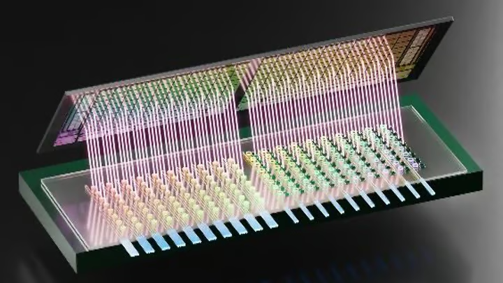
Photons (light)
Massless and chargeless, photons travel at high speed with minimal loss. They support extreme bandwidth through wavelength-division multiplexing (WDM), and don’t suffer resistance, capacitance, or crosstalk. But they’re hard to use for logic — photons don’t naturally interact — so most systems convert light back to electrons for computation.
Phonons (vibrations)
Bits carried by mechanical vibration — essentially sound. Once used in early delay-line memory and still useful in analog signal processing. But they’re far too slow and lossy for general-purpose compute, and tend to dissipate energy as heat through friction.
Magnons (spin waves)
These propagate as ripples in magnetic materials — waves of spin rather than current. They can theoretically reduce energy loss compared to moving charge, and show promise in spintronic logic. But they remain experimental, with poor scalability and limited integration with existing silicon systems.
Fluidic and biological carriers (molecules)
Computing with chemicals, microfluids, or DNA. These systems shine in specialized domains — massively parallel DNA reactions, biochemical sensing — but are wildly slower than electronics and fundamentally unsuited for high-speed digital logic.
So, in theory, you can build computers from many different kinds of carriers. But of all these, only photons combine the right physics with growing commercial maturity.
We already use them everywhere data needs to travel: undersea cables, inter-datacenter links, even rack-scale optics in modern hyperscale clusters. Photons can carry terabits per second through a single fiber strand, using color (wavelength), polarization, and spatial mode to pack multiple channels into one medium. And thanks to decades of investment in telecom infrastructure and silicon photonics, we’re starting to integrate them directly onto chips.
Why photons win:
- Speed: They travel at light-speed (in fiber: ~5 inches per nanosecond)
- Efficiency: Optical links consume just 1–2 picojoules per bit — 10–50× better than copper
- Parallelism: One fiber can carry 100+ channels simultaneously with no interference
There’s no free lunch. Generating and detecting photons at chip-scale remains challenging. Photonic logic gates require nonlinear materials or conversion back to electrons. And the ecosystem is still slowly spinning up, from design tools to packaging to thermal tuning.
But these are solvable engineering problems, not physics barriers.
The question isn’t whether photons can move data more efficiently — it’s how quickly we can re-architect systems to take advantage.
Electrons gave us the industrial internet.
Photons are poised to power the cognitive one.
Section 003
Photonic architecture movement
If this is a new epoch, it demands a new design language — and new materials to match. In computing, we’re at the edge of an architectural shift as significant as masonry to steel, or analog to digital. Photonics is no longer confined to theory papers and controlled lab demos.
Much like architectural movements in building design often spring from multiple cultural centers (think Bauhaus in Europe, skyscrapers in Chicago, and so on), across the globe, scientists, engineers, governments, and startups are racing to move light from the fringe to the foundation of compute.
What was once speculative is hardening into systems. Real chips. Real packaging. Real production pipelines. The movement is global — Boston, Silicon Valley, Shanghai, Berlin, Oxford, Seoul, Tel Aviv — each building a different part of the future stack. Momentum is strong and concentrated in the U.S., where a surge of well-capitalized startups (and industry mainstays) are working to push photonics out of the lab.
The United States
Some are rethinking inference. Others are tearing down the memory wall, embedding co-packaged optics, or redesigning the rack itself. Each one attacks the electron bottleneck from a different vector — but all are betting on light. There are (at least) six to know: Lightmatter, Celestial AI, Luminous Computing, Ayar Labs, Lightintelligence, and Anello Photonics.
Explore the landscape ↓
Big Tech (and Big Chip)
Beyond startups, major U.S. players are quietly laying optical groundwork. Intel has a long-running silicon photonics program, with optical transceivers already integrated on motherboards and exploratory work underway on optical memory interconnects. Hyperscalers like Meta, Microsoft, and Google are actively researching and deploying optical fabrics for AI infrastructure.
Intel has shipped 8M+ silicon photonic transceivers, with 32M+ on-chip lasers, and last year unveiled its OCI chiplet: a fully integrated optical I/O solution that can be co-packaged with CPUs and GPUs, delivering up to 4 Tbps of bandwidth at a fraction of the power of traditional electrical links. At the same time, NVIDIA is advancing the field with its new Spectrum-X and Quantum-X silicon photonics switches, integrating co-packaged optics to connect millions of GPUs at hyperscale, and delivering 3.5x higher power efficiency and 10x better network resiliency than legacy approaches.
In 2023, Google revealed it had rolled out thousands of custom 136-port MEMS-based optical circuit switches across its data centers — a core part of its Apollo project — replacing traditional electrical spine networks. Google attributed serious improvements to its custom network architecture: 30% higher throughput, 40% lower power use, 30% lower capex, 10% faster flow completion, and 50x less downtime.
Meta is pushing the envelope, too, and working to build out large-scale optical switching fabrics for its next-gen AI clusters. The company is actively testing MEMS-based optical circuit switches and robotic fiber patch panels to dynamically rewire GPU connectivity in real time, targeting 30–40% lower network power and microsecond-scale reconfiguration for massive clusters.
Microsoft, for its part, is investing in next-generation optical technologies like hollow core fiber to accelerate AI workloads and expanding its datacenter backbone with new fiber-rich private connectivity fabrics. And not to be outdone, AWS is ramping up its own investments in advanced optical interconnects and private fiber networks and is rumored to be exploring photonic memory pooling architectures, as it rolls out massive new campuses to keep pace with ever-larger models.
The signal across the board: photonics is no longer a curiosity — it’s becoming a core layer of future hyperscale architecture.
Meanwhile, in china…
China’s photonics effort is as much top-down as bottom-up. Strategic pressure from chip restrictions has accelerated state investment, but the groundwork was already there: labs, talent, ambition, and photonics call-outs in five-year plans. A key milestone came in late 2024 with the launch of China’s first state-backed photonic chip pilot line in Wuxi, affiliated with Shanghai Jiao Tong University. Designed to produce up to 10,000 wafers annually, the foundry supports key materials like silicon photonics, silicon nitride, and lithium niobate on insulator (LiNbO₃), a standout for high-speed modulators. PDKs (process design kits) are slated for imminent release, signaling an ambition not just to prototype, but to scale — laying groundwork for a national photonics industry, much like TSMC did for semiconductors in Taiwan.
On the academic front, Chinese universities are hitting global benchmarks. In 2023, a Tsinghua-led team introduced the ACCEL chip — a fully analog optical processor that reportedly outperformed NVIDIA’s A100 on certain computer vision tasks at far lower power, despite being built on an ancient 180 nm process. That same year, Tsinghua unveiled its “Taiji” chip for optical neural network training, while Peking University demonstrated a fully programmable photonic topological chip integrating thousands of optical components. These projects reveal that China is attacking photonics from multiple fronts: both application-specific optical accelerators and more general-purpose, programmable photonic processors.
The strategy is clear: build the fabs, fund the science, back the companies, and bake photonics into national long-term compute infrastructure. This is a familiar playbook: identify a foundational technology where the West is encumbered by legacy, then leapfrog.
China did it with 5G — moving early, investing heavily, nurturing a champion (Huawei), and outpacing rivals in R&D and deployment while shaping global standards. You’ve seen the same playbook with photovoltaics, EVs, high-speed rail, and battery manufacturing — targeting sectors where technological transition levels the playing field and legacy advantage becomes baggage.
We’re in a moment where the dominant architecture (electrons and copper) is hitting physical limits, and a new material regime (light) is still up for grabs. In the logic of Made in China 2025, this is a textbook leapfrog window — get in early, build industrial capacity, and close the gap before others can retool. If the post-silicon era is defined by bandwidth, latency, and energy efficiency, then photons — and the ability to manufacture, package, and deploy them at scale — may become a cornerstones of compute sovereignty.
European efforts
Europe’s tech sector, the butt of many jokes from Silicon Valley and social media pundits, punches above its weight in photonics, thanks to a deep research base, an emerging wave of startups, and a growing foundry ecosystem.
- Salience Labs recently launched what it calls the first commercial photonic computing module: a PCIe accelerator that uses thin-film lithium niobate to perform matrix multiplications and nonlinear transforms. One beam of light can replace thousands of transistors for analog math — no heat, no switching overhead. Salience, with $30M in backing, is targeting ultra-high-bandwidth photonic switching — essentially an optical NVSwitch.
- In the U.K., Optalysys and Lumai (a spin-out from Oxford) are also pushing novel co-processors and interconnects. Lumai raised $10M+ this year for its radical free-space optics approach to matrix ops.
- France’s LightOn, meanwhile, has taken a different path: pioneering random projection-based inference with off-the-shelf optical setups, deployed on cloud platforms as early as 2019.
At the research level, European institutions are powerhouses in photonics. IMEC (Belgium) leads on neuromorphic and silicon photonics R&D. The University of Münster set speed records for optical matrix multiplication. Horizon-funded initiatives like Photonics21 and NEUROPhotonics have helped seed pan-European collaboration. Foundry access — via GlobalFoundries (Dresden), STMicroelectronics, Tower Semiconductor, and others — gives startups a way to actually build chips, not just model them.
Europe may not have a flagship program or a megastack startup, but its range and momentum in photonics are undeniable.
Elsewhere in the world
Outside of the big three, photonic computing is gaining momentum across the globe:
- Canada: Xanadu leads in quantum photonics, developing modular, room-temperature photonic quantum computers on silicon platforms (technology that could ultimately spill into classical high-speed computing as well).
- Israel: Tower Semiconductor is a major global foundry for silicon photonics, offering high-volume manufacturing and advanced process design kits for optical interconnects.
- Japan: NTT Research has demonstrated photonic circuits that solve complex optimization problems—like Ising models—using hybrid classical-quantum photonic architectures
- Australia: Researchers are developing microwave photonics chips for ultrafast analog signal processing and computation, leveraging thin-film lithium niobate for speeds and efficiency far beyond traditional electronics.
- Legacy tech giants: IBM, HP/HPE, and other established players continue to seed the photonics space through internal R&D, strategic investments, and alumni-led spinouts. For example, HPE has partnered with Ayar Labs to develop next-generation silicon photonics solutions for HPC and AI workloads.
All told, this is the early phase of a global architectural shift.
The pieces — innovative startups, national fabs, academic breakthroughs, commercial traction — are falling into place. We haven’t yet seen the photonic equivalent of IBM’s System/360 (a platform standard) or Intel’s 4004 (a breakout chip that catalyzes an ecosystem), but the activity is unmistakably building. Photonics is moving from research demos into deployed systems, from lab bets into infrastructure plays.
As of 2025, light-based computing isn’t mainstream. But it’s no longer speculative either. The movement is real, it’s growing, and it’s beginning to prove itself in high-value niches. The tipping point hasn’t arrived — but it’s starting to come into view.
The sections that follow explore what’s still missing: the blockers, bottlenecks, and breakthroughs needed to push photonics from promise to dominance — and what it would mean to finally compute at the speed of light.
Section 004
The commercialization curve: Where photonics is — and isn’t — completely ready
If photonic technology is so compelling, one might ask, why hasn’t it taken over already? Silicon electrons have had a decades-long run; what’s preventing photons from sweeping in and replacing electronic systems wholesale?
The answer lies in a mix of physics, manufacturing realities, and good ole’ ecosystem inertia. From relays to tubes, tubes to transistors, transistors to integrated circuits, single-core to multi-core, and more, every paradigm shift in computing was limited not by imagination, but by integration.
Photonics, for all its advantages, has to fight its way through an installed base and an ingrained mindset built around electronics. This section examines what’s not ready yet, or where breakthroughs are most needed, to fully unleash photonics’ potential in AI infrastructure.
001 / Manufacturing, Fabrication, and the Precision
Modern CMOS fabs are marvels of precision, spitting out billions of near-perfect transistors at single-digit-nanometer nodes and >90% yields. Producing photonics devices has historically been larger and more scattershot (a single waveguide is still measured in microns, and a few nanometers of etch error can shift its refractive index enough to break a circuit). Worse, the stack is multi-material: silicon for logic, indium-phosphide for lasers, silicon nitride or LiNbO₃ for modulators. Those layers don’t flow through a vanilla CMOS tool-chain, so yields are lower and costs higher.
No TSMC-for-light exists yet. Instead, we have a patchwork of specialty lines (GlobalFoundries, Tower, AIM, IMEC, a new state-backed fab in Wuxi) and each has its own quirks. Progress is real: GF now ships an open photonics PDK, while Intel already integrates 100 G optical transceivers at scale. Still, the ecosystem remains the Wild West. A photonic tape-out often needs multiple shuttles and bespoke tuning before volume.
Breakthrough requirement: semiconductor-like (CMOS-grade) repeatability:
- Process: monolithic flows that bond III-V lasers or LiNbO₃ modulators to silicon in one pass.
- Design: on-chip phase shifters and heaters to trim away fab variability.
- Assembly: co-packaged optics that let each die run its own optimal process, then stitch together in-package.
Until manufacturability matures, photonic hardware won’t be turnkey. We believe it’s roughly a decade behind electronics on the learning curve. But every new pilot line, PDK, and co-packaged demo narrows the gap. And manufacturability will be the lever that moves the rest of the curve.
002 / Packaging and Integration: The Alignment Problem
Making a great photonic die is only half the job; getting light in and out is the harder half. Electrical chips are packaged by the million with pick-and-place robots and solder balls. Photonic dies must mate with fibers or on-package lasers at sub-micron alignment. Imagine trying to align a human hair (optical fiber) to a waveguide just a few microns wide on a chip, and repeating this for ~64 fibers per chip, with tolerances of a fraction of a micron to minimize loss. This is hard.
Today it’s often done with active alignment (using feedback from the optical signal) and is not easily scalable. Furthermore, photonic chips tend to be larger, and when you combine them with electronics (like a photonic compute chip with a CMOS driver/reader chip), you have a heterogeneous assembly that can be tricky to package thermally and mechanically.
Scale is coming, but the tooling isn’t turnkey yet.
- Co-packaged optics: Intel and Ayar Labs now “butt-couple” fiber ribbons to micro-lenses etched on the die, shipping 4 Tb/s modules that drop straight onto a board.
- On-board lasers: PICs with bonded III-V gain sections remove the external laser can, but add thermal and materials complexity.
- Printed polymer waveguides: companies like CelLink and Samtec are testing flexible light-guides that route photonics over the package surface — no fiber ferrules needed.
Breakthrough requirement: turn photonic packaging into true plug-and-play — snap-fit fiber alignment, standard drop-in lasers, and built-in thermal tuning — so light-based chips can run down the same automated lines that assemble GPUs today.
When a photonic die can be flipped, under-filled, and fiber-mated on the same line that handles GPUs, the adoption curve bends sharply upward. Until then, packaging remains a bottleneck between promising prototypes and datacenter volume.
003 / Software and System Integration: Drop-in or Die
Let’s assume for a moment we’ve solved the hardware challenges, and that we can manufacture and package working photonic systems at scale. As hardware hurdles fall, the next hill is getting a finicky bunch — system designers and software engineers — to adopt your technology.
- AI infrastructure runs on GPUs, DPUs, and CPUs (all electronic systems).
- Today’s AI stack — CUDA, TensorFlow, PCIe drivers, CXL fabrics — assumes certain hardware paradigms (e.g., it was written for electrons).
- Every layer of the stack expects electrons and GPU-style timing. Drop a photonic accelerator into that world and nothing recognizes it: kernels expect floating-point behavior, schedulers assume GPU latencies, and network layers treat light like an exotic visitor.
The path to relevance is the GPU playbook, rewritten for photons: appear as just another device on the bus, load with stock drivers, and plug into existing frameworks. In the 2000s, NVIDIA won not just by fielding best-in-class FLOPS, but by doing exactly this, and allowing devs to port models in a weekend. Photonics needs the same glide path. A photonic card must enumerate like a GPU, surface a familiar API, and return the right answers inside existing tolerance windows…no rewrites, no exotic data types.
Breakthrough requirement: a drop-in photonic card that shows up like any GPU, ships with turnkey drivers and toolchains, reports laser health as easily as temperature, and demonstrates clear $/FLOP and watt savings at cloud scale.
Lightmatter’s Envise leans hard into that model: shipping translator tools that map TensorFlow graphs onto its photonic cores. This can mean the difference between “cool demo” and capex line-item. But, by and large, we’re not there yet. Using today’s photonic accelerators often involves adapting algorithms to analog computing quirks or dealing with lower precision. It’s doable for adventurous early users, but not for the mainstream.
004 / Cultural and Commercial Readiness: Scaling Light’s S-curve
Imagine wheeling a photonic board into a modern rack. The silicon is flawless, the packaging airtight — and the firmware prompt still reads Unknown Device. Ops engineers have already been peppering you with unglamorous questions:
- Will lasers drift off spec?
- Can our monitoring tools see inside the package?
- How do we scrape optical power?
- What’s the MTBF of a grating coupler at 35 °C?
- What happens at 4 a.m. when a fiber coupler unseats?
A cloud operator who lives by five-nines uptime (and is paid to avoid downtime) is not about to rewrite the inference pipeline for a niche card that looks exotic, requires custom math and hand-tuned drivers; speaks a private dialect, and offers no tooling safety net.
As we’ve already established above, software parity is table stakes. Reliability, monitoring, and vendor support are also key guardrails. Tooling is catching up (Prometheus hooks for laser health, CXL lanes that treat light as a first-class citizen, compilers that quantize around analog noise floors) but most continue to evolve.
None of this is exotic; it’s the plumbing work that followed every new accelerator class (GPUs, and TPUs, too). But until photonics proves boringly reliable — and economically superior — most clouds will watch from the sidelines.
Breakthrough requirement: A single flagship deployment, proving reliability and publicly saving megawatts and dollars, flips the risk ledger overnight.
The inflection point will come as a press release that changes everything: “We trained GPT-N 20% faster and pulled 30% less power, because half the math ran on photonic accelerators.” We have many hints (explored above) that Big Tech is angling for this inflection, but the watershed announcement hasn’t landed. But mark our words: when an AWS-scale player declares, “This rack trains faster and costs less because it runs on light,” the rest of the field will follow.
005 / Talent, skills and tooling: The human bottleneck
Silicon design commands a workforce in the millions, while integrated photonics could still fit in a football stadium. Only a few thousand engineers worldwide can route a dense waveguide mesh, align on-chip lasers, and model phase drift without breaking sweat. The toolchain reflects that scarcity: CMOS EDA can time-close a billion-transistor SoC; photonic EDA still juggles bespoke models for loss, polarization, and thermal tuning.
Big Tech feels the pinch. When a hyperscaler launches an optics program, it may struggle to find enough seasoned photonics folks to hire — and instead look to acquire (read: acqui-hire) a startup to pad out its talent bench with a half-dozen specialists. Yes, companies like Synopsys and Cadence are now bundling photonics design module plug-ins to their suites, and universities are minting more optics PhDs, but the ramp remains steep.
The fix is largely pedagogical (plus being patient).
Programs like AIM Photonics Academy (U.S.) and PhotonHub (EU) are pushing waveguide labs into sophomore EE courses; open PDK shuttles let students tape out a test die for pocket change; and every new reference library helps turn optics every new reference library turns optics into “drag-and-drop”— less wizardry, more worksheet. Process standardization and design kits will also lower the barrier so that one doesn’t need a PhD in optics to include a photonic block in a system design. Slowly but surely, each shuttle, each lab kit, makes optics a little less exotic and a little more “drag-and-drop.”
Breakthrough requirement: grow the photonics talent pool from stadium to city, with enough coursework, tooling, and mentorship to mint tens of thousands of optical designers, not thousands. The goal is to make photonics boring — in the best sense — as a standard part of the toolbox, taught in undergrad engineering, supported by vendor libraries, and so on.
GPUs followed the same arc: once a dark art and occult skill, now a standard elective. Give photonics that same glide slope — cheap tools, open libraries, clear career ladders — and light stops being a curiosity and starts becoming a default design block.
On the cusp: toward photonic architecture
Copper is starting to choke the datacenter: rising clock rates push links into tens of picojoules per bit, and the cooling bill is edging toward the power bill. That pain is why hyperscalers are already trial-running optical circuit switches, co-packaged optics, and memory fabrics — anything that swaps electrons for light in the loudest, hottest lanes.
Think of photonics today like EVs circa 2015: proven on the test track, waiting for the cost curve to bend and the charging (read: packaging and software) network to fill in. When skyrocketing bandwidth demand meets surging energy prices, photons jump from “nice to have” to “mandatory retrofit.”
The first wins are surgical. Cisco, Broadcom, and several HPC labs now demo switch backplanes and CPU-GPU interconnects that move data at 4 Tb/s with single-digit picojoule budgets. These drop-in links cut power without forcing software changes — the medium flips from copper to glass, but Ethernet and PCIe packets don’t care.
Full photonic computing is tougher (see: noise floors, resonator Q, optical memory), so companies like Lightmatter and Q.ANT run the heavy math in light but keep control logic in silicon. It’s hybrid by design. Harvest optical energy efficiency where it’s easy, and let electrons do what they still do best.
Picture the commercialization curve as an uphill grade: manufacturing, packaging, standards, skills. Each is a steep stretch. Year by year the slope eases, and once those switchbacks are behind us, the climb to mass adoption will accelerate.
We won’t bulldoze the electron infrastructure we’ve built; we’ll braid photons into it, inching light ever closer to the compute core. As an IBM researcher quipped, “Photonics won’t displace electronics; it will embrace it.” In the next section we’ll sketch that coming hybrid — where copper, silicon, and glass share the motherboard — and show how it could reshape the entire language of system design.
Section 005
Light as form: The Architecture of AI’s future
Every architectural movement has a tipping point, when materials, constraints, and opinions converge into a new design language.
Reinforced concrete liberated Frank Lloyd Wright to cantilever Fallingwater over a torrent, and later let engineers float free-form stadium roofs that seemed to defy gravity. Aluminum turned aircraft from fabric kites into globe-spanning pressurized tubes.
If steel lifted cities into the sky, silicon let engineers escape scale. In computing, vacuum tubes filled gymnasiums until the silicon transistor shrank logic onto a fingernail, and the printed-circuit board stitched those fingernails into modular systems that could be serviced like Lego.
Photonics promise the next phase change.
But we must think in optical form, not optical devices. When light is the motherboard’s native language, distance behaves like it does in long-haul fiber: nearly free. Boards can sprawl like airport concourses, joined by luminous moving walkways. Memory vaults slide two aisles away yet feel electrically next door. Cooling shifts from firefighting a furnace to venting warm across a quiet atrium. A future technician could trace faults the way a conservator follows cracks in stained glass: by spotting which wavelength goes dark against a glowing backplane.
Light doesn’t just relax old limits; it hands the architect a fresh canvas, as radical as the first steel girder or printed-circuit board. So the closing question of today’s antimemo is: How will a substrate of pure light — erasing distance, diffusing heat, slimming infrastructure, and initially playing second fiddle to silicon — re-architect the machinery, the economics, and ultimately the geography of AI?
From Component to System
For two decades, modular computing has lived on copper leashes. We kept slicing machines into finer pieces (multicore CPUs, chiplets, GPU pods, disaggregated memory), but every slice still had to sit within a few hot-and-bothered centimeters of its neighbor.
Distance and topology are dictated by electrons: stretch a trace, lose energy; add a hop, add latency. Motherboards shrank into dense islands, racks became cable mazes, datacenter aisles narrowed around heat sinks the size of suitcases. What passed for modularity was really an architecture of proximity and hierarchy enforced by electrical limits.
Photonics cuts those limits at the root. With photonic links, the cost — latency, energy, repeaters, layout grief — of 2 cm, 2 m, or even 200 m is nearly indistinguishable.
Topology, then, becomes a software choice. A processor can tap any memory pool or any peer and still see single-digit–nanosecond delays. Massive optical backplanes let CPUs, memory bricks, and accelerators snap in like LEGO, their ports stitched by light instead of pin-limited sockets.
Need to “wire” 16 GPUs for one training phase and 64 for the next? An optical fabric can reroute paths in micro-seconds. Suddenly, a CPU complex can talk to a memory vault three racks away as if it were soldered on the same board. Resources re-organize by logical needs rather than physical adjacency: spin up a giant context window, borrow a terabyte pool on demand; conjure an RL swarm, lash fifty GPUs into a transient mesh, then dissolve it when the episode ends…no rewiring required!
This vision has a shape: disaggregated memory, cohered by light. Entire racks could operate as a single, coherent compute fabric, a vision gestured at by HPE’s “The Machine” and now advanced by Ayar Labs and Intel’s optical interposers.
From Heat to Harmony
Copper’s losses turned servers into space heaters. Push electrons fast enough and you pay twice: first in I²R losses that bloom into waste heat, then in the fans and chillers that swallow up to half of your datacenter’s power budget. Photonics break that loop. Light slips through glass without joule-to-heat penalties, so interconnect energy collapses and thermals no longer dictate the floorplan.
Picture the same 400 W of compute, but scattered as four 100 W photonic tiles across a chassis, each sipping cool air instead of begging for a turbine. Stretch that idea to the rack: accelerators on one shelf, high-bandwidth memory two shelves up, laser sources tucked near the power plane — all linked by waveguides that add nanoseconds, not hotspots. Heat is no longer a point load; it’s a low, even glow you can vent gently.
Vertical design opens next. In a 3D stack, optical connectors haul bits — and thermal flux — straight upward. Columbia’s recent test die ran 800 Gb/s through 80 on-stack transceivers at just 120 fJ/bit, hinting at volumetric architectures where z-axis bandwidth equals x-y, and temperature spreads like light itself.
That pattern isn’t mechanical; it’s biological. Vascular networks diffuse heat and nutrients through branching capillaries; photonic fabrics can do the same for data and joules, feeding every “organ” without frying the core. The result is distributed thermal design: heat is spread, not concentrated. Smoother thermals extend silicon life, slash cooling capex, and let architects place compute for logic’s sake, not coolant’s. When light shoulders the traffic, the datacenter stops fighting physics and starts flowing with it — information and energy circulating in quiet harmony, much like a living system.
A New Design Ethos
Light invites cleaner hardware. A transparent fiber-optic backplane wears its arteries on the outside, the way Eiffel flaunted iron trusses in Paris.
Remove copper’s losses and the clutter goes with it: no bundles of cable spaghetti, no dark raceways to trace when something fails. A rack can announce its purpose visually: slender waveguides pulse magenta when a model trains, sapphire blue when an epoch checkpoints, amber when a memory vault spins up. The cabling nightmare melts into a quiet, luminous lattice. You can read the rack at a glance.
Legibility isn’t cosmetic, it’s uptime. An optical backplane treats every slot as address-agnostic: slide in a compute tile, a DRAM brick, or a laser pump and the mesh reroutes in microseconds. No pin-budget gymnastics, no electromagnetic interference (EMI) shielding, no scorched fingers from point-hot devices.
- Could cables go next? Research labs and a few bold hyperscalers are testing fingertip-sized mirrors that aim laser beams straight from chip to chip, or rack to rack, letting data ride on open air instead of fiber and stripping yet another layer of friction from the system.
Modularity follows clarity. Standardized photonic ports promise upgrades that feel like LEGO — snap out an aging accelerator, pop in its optical heir, and the fabric absorbs it with no recabling. Light neither radiates nor listens, so ground planes, ferrite beads, and thick dielectrics fade away, slimming boards and easing airflow. Cooling, too, turns elegant: passive liquid plates shimmer behind clear manifolds, heat diffused instead of battled.
Form now follows photonics. Distance dissolves, noise quiets, and infrastructure sheds bulk. What remains is a datacenter written not in copper snakes and roaring turbines, but in silent lines of light: a new design ethos for the age of AI.
Not a Revolution, but a Realignment
To advocate for data riding on photons does not make us partisans of a coup d’état against electrons. Instead, this is a steel-frame moment, when a new material slips into the structure and quietly changes everything.
We’ll still lean on electrons for dense logic, tight caches, and the nonstop Boolean grind. Photons will handle motion, shuttling data at light-speed and light-heat, and living up to their name (phōs, Greek for “light”), as nature’s original express courier. Wherever bandwidth, fan-outs, and certain parallel analog tricks matter, optics will sprint past copper and never look back.
So, if the winning stack is opto-electronic, what might this mixed substrate future look like on the workbench? Early glimmers of a brave new age excite:
- NVIDIA’s Grace Hopper superchip still speaks in copper dialectic today, but we imagine a next-gen GH200 could laser-link the CPU and GPU right on the module.
- Intel’s Ponte Vecchio GPU uses EMIB and Foveros (electronics packaging) for now, yet an optical interposer seems like a logical sequel.
- In memory, we may see DRAM modules with optical read/write interfaces, letting racks share a coherent pool without drowning in I/O heat.
None of this is fantasy; it’s a node or two removed from us today. And the realignment is already underway: from prototype supercomputers routing node-to-node traffic through fiber, to experimental chips laying holographic optics atop CMOS to off-load dense math. Nobody is scrapping decades of transistor craft — they’re adding light the way Bauhaus architects showcased raw steel and glass: honest function, no excess ornament.
The future belongs to architects who weave substrates. Heterogeneous compute will win not as a zoo of electronic accelerators, but as seamless fabric of optical interconnects, photonic tensor engines, co-packaged electro-optic chips, and the like. When silicon and light share the stage, in a tightly tuned concerto of computation, pure-play dogmas will one day feel brittle.
Steel never banished brick; it simply shifted the load so brick could become façade. Photons will do the heavy lifting of bandwidth, leaving electrons free to keep crunching at atomic scales.
The will of our epoch
In the introduction we borrowed Mies’s line that architecture is the will of an epoch translated into space. Our epoch’s will is a hunger for intelligence in silico at planetary scale. That desire demands machines that scale without buckling, sip energy instead of gulping it, and re-arrange themselves on the fly. Photonics, more than any other ingredient now on the table, lets us chase all three.
Light rewrites the boundaries of the possible. It slashes the cost of distance, mutes the roar of cooling, and frees topologies to arrange themselves around ideas rather than heat sinks. The very space of computation is being reshaped: walls of distance and bandwidth are coming down, while new structures of light and silicon rise in their place.
Consider this antimemo an ode to photons. But it need not be an elegy for electrons. These faithful workers will continue crunching logic in nanometer caverns, with photons freeing them from having to ferry this logic across vast oceans of data.
Decades from now — when historians scroll through schematics instead of cathedral floor plans — they may tag the tail end of the 2020s when the light came on: the moment lasers and waveguides flooded the datacenter, and compute infrastructure took on a new, unmistakable form.
Look closely and you can already see that form emerging: laser-linked clusters; modular AI fabrics; radiant silicon interposers carrying torrents of data. Walls of distance and bandwidth are falling. In their place rise airy lattices of photons and electrons, hardware and code co-designed, thermals and networks held in delicate balance.
The outline is faint but certain, like steel ribs rising from a muddy foundation before a skyscraper takes shape. When the age of photonic computing dawns, and when light and silicon carry our intelligence forward at full noon, we’ll recognize the moment the way past generations recognized the first spark of electric light or the first flight of aluminum wings.
The architecture of AI’s future will be built of photons and electrons, of hardware and code co-designed, of thermal and network balance: an architecture not of rigid hierarchies but of fluid light and form.
The future architecture of AI, taking shape today in lab demos and first-gen products, is our cathedral in the making — built not of stone and stained glass, but of waveguides and wavelengths — for the epoch of insatiable intelligence, illuminated by light.